Előadást letölteni
Az előadás letöltése folymat van. Kérjük, várjon

1
Többmagos/sokmagos processzorok-2
Sima Dezső 2013 Március Version 1.2

2
Áttekintés 1. Többmagos processzorok megjelenésének szükségszerűsége
2. Homogén többmagos processzorok 2.1 Hagyományos többmagos processzorok 2.2 Sokmagos processzorok 3. Heterogén többmagos processzorok 3.1 Mester/szolga elvű többmagos processzorok 3.2 Csatolt többmagos processzorok 4. Kitekintés

3
3. Heterogén többmagos processzorok

4
3. Heterogén többmagos processzorok (1)
Multicore processors Homogenous multicores Heterogenous multicores Conventional MC processors Manycore processors Master/slave architectures Add-on architectures 2 ≤ n ≤ 8 cores with >8 cores Desktops Servers MPC CPU GPU General purpose computing Prototypes/ experimental systems MM/3D/HPC production stage HPC near future 3.1 ábra Többmagos processzorok főbb osztályai

5
3.1 Heterogén többmagos mester/szolga elvű TP-ok
A Cell processzor

6
3.1 Heterogén mester/szolga elvű TP-ok - A Cell (1)
Cell BE Sony, IBM és Toshiba közös terméke Cél: Játékok/multimédia, HPC alkalmazások Playstation 3 (PS3) QS2x Blade Szerver család (2 Cell BE/blade) Előzmények: 2000 nyara: Az architektúra alapjainak meghatározása 02/2006: Cell Blade QS20 08/ Cell Blade QS21 05/ Cell Blade QS22
 QS2x Blade Szerver család. (2 Cell BE/blade) Előzmények: 2000 nyara: Az architektúra alapjainak meghatározása. 02/2006: Cell Blade QS20. 08/ 2007 Cell Blade QS21. 05/ 2008 Cell Blade QS22.")
7
3.1 Heterogén mester/szolga elvű TP-ok - A Cell (2)
SPE: Synergistic Procesing Element SPU: Synergistic Processor Unit SXU: Synergistic Execution Unit LS: Local Store of 256 KB SMF: Synergistic Mem. Flow Unit EIB: Element Interface Bus PPE: Power Processing Element PPU: Power Processing Unit PXU: POWER Execution Unit MIC: Memory Interface Contr. BIC: Bus Interface Contr. XDR: Rambus DRAM 3.1.1 ábra: A Cell BE blokk diagramja [1]

8
3.1 Heterogén mester/szolga elvű TP-ok - A Cell (3)
3.1.2 ábra: A Cell BE lapka (221mm2, 234 mtrs) [1]
 [1]")
9
3.1 Heterogén mester/szolga elvű TP-ok - A Cell (4)
3.1.3 ábra: A Cell BE lapka – EIB [1]

10
3.1 Heterogén mester/szolga elvű TP-ok - A Cell (5)
3.1.4 ábra: Az EIB működési elve [1]

11
3.1 Heterogén mester/szolga elvű TP-ok - A Cell (6)
3.1.5 ábra: Konkurens átvitelek az EIB-en [1]

12
3.1 Heterogén mester/szolga elvű TP-ok - A Cell (7)
Példa egy komplex alkalmazás futtatása (digitális TV dekódolása) a Cell processzoron [2]
 a Cell processzoron [2]")
13
3.1 Heterogén mester/szolga elvű TP-ok - A Cell (8)
A Cell teljesítménye és a NIK részvétele a Cell teljesítmény-vizsgálataiban 3.2 GHz: QS21 Csúcs SP FP: 409,6 GFlops (3.2 GHz x 2x8 SPE x 2x4 SP FP/cycle) Cell BE - NIK 2007: Faculty Award (Cell 3Đ app./Teaching) 2008: IBM – NIK Kutatási Együttműködési Szerződés: Teljesítményvizsgálatok IBM Böblingen Lab IBM Austin Lab
 Cell BE - NIK. 2007: Faculty Award (Cell 3Đ app./Teaching) 2008: IBM – NIK Kutatási Együttműködési Szerződés: Teljesítményvizsgálatok. IBM Böblingen Lab. IBM Austin Lab.")
14
3.1 Heterogén mester/szolga elvű TP-ok - A Cell (9)
The Roadrunner 6/2008 : International Supercomputing Conference, Dresden A világ 500 leggyorsabb számítógépe listáján (Top500): 1. Roadrunner 1 Petaflops (1015) fenntartott teljesítmény (Linpack)
: 1. Roadrunner. 1 Petaflops (1015) fenntartott teljesítmény (Linpack)")
15
3.1 Heterogén mester/szolga elvű TP-ok - A Cell (10)
3.1.6 ábra:A világ leggyorsabb számítógépe: IBM Roadrunner (Los Alamos 2008) [3]
 [3]")
16
3.1 Heterogén mester/szolga elvű TP-ok - A Cell (11)
3.1.7 ábra: A Roadrunner főbb jellemzői [1]

17
3.2 Heterogén csatolt többmagos processzorok

18
3.2 Heterogén csatolt többmagos processzorok (1)
Multicore processors Homogenous multicores Heterogenous multicores Conventional MC processors Manycore processors Master/slave architectures Add-on architectures 2 ≤ n ≤ 8 cores with >8 cores Desktops Servers MPC CPU GPU General purpose computing Prototypes/ experimental systems MM/3D/HPC production stage HPC near future 3.2.1 ábra: Többmagos processzorok főbb jellemzői

19
3.2 Heterogén csatolt többmagos processzorok (2)
Csatolt elvű végrehajtás elve GPGPU-k esetén (a legegyszerűbb (kötegelt) szervezést feltételezve) [4] Host Device kernel0<<<>>>() (Adatpárh. progr.) kernel1<<<>>>()
 szervezést. feltételezve) [4] Host. Device. kernel0<<<>>>() (Adatpárh. progr.) kernel1<<<>>>()")
20
3.2 Heterogén csatolt többmagos processzorok (3)
Megjegyzés a működési elvhez Heterogén csatolt többmagos processzorok: feldolgozás gyorsítók (accelerators) A működési elv szempontjából előzmény: heterogén csatolt társprocesszoros rendszerek Példák: korai személyi számítógépek lebegőpontos társprocesszorokkal Intel Az Intel 486-nak már volt saját “on-chip” lebegőpontos egysége (FPU) (az SX és SL modelek kivételével)
 A működési elv szempontjából előzmény: heterogén csatolt társprocesszoros rendszerek. Példák: korai személyi számítógépek lebegőpontos társprocesszorokkal. Intel Az Intel 486-nak már volt saját on-chip lebegőpontos egysége (FPU) (az SX és SL modelek kivételével)")
21
Heterogén csatolt többmagos processzorok
Heterogén csatolt többmagos processzorok legfontosabb implementációi Heterogén csatolt többmagos processzorok Integrált grafika Okostelefonok

22
3.2.1 Az Integrált grafika megjelenése

23
3.2.1 Az Integrált grafika megjelenése (1)
Áttérés angol nyelvű slide-ok használatára

24
3.2.1 Az Integrált grafika megjelenése (2)
Implementation of integrated graphics Implementation of integrated graphics In the north bridge In a multi-chip processor package on a separate die On the processor die Both the CPU and the GPU are on separate dies and are mounted into a single package P South Bridge Mem. NB IG South Bridge Mem. NB P GPU CPU Periph. Contr. Mem. CPU GPU P Implementations about Intel’s Havendale (DT) and Auburndale (M) (scheduled for 1H/2009 but cancelled) Arrandale (DT, 1/2010) and Clarkdale (M, 1/2010) Intel’s Sandy Bridge (1/2011) and Ivy Bridge (4/2012) AMD’s Swift (scheduled for 2009 but canceled) AMD’s Bobcat-based APUs (M, 1/2011) Llano APUs (DT, 6/2011) Trinity APUs (DT, Q4/2012)
 and. Auburndale (M) (scheduled for 1H/2009. but cancelled) Arrandale (DT, 1/2010) and. Clarkdale (M, 1/2010) Intel’s Sandy Bridge (1/2011) and. Ivy Bridge (4/2012) AMD’s Swift (scheduled for but canceled) AMD’s Bobcat-based APUs (M, 1/2011) Llano APUs (DT, 6/2011) Trinity APUs (DT, Q4/2012)")
25
3.2.1 Az Integrált grafika megjelenése (3)
Implementation of integrated graphics Implementation of integrated graphics In the north bridge In a multi-chip processor package on a separate die On the processor die Both the CPU and the GPU are on separate dies and are mounted into a single package P South Bridge Mem. NB IG South Bridge Mem. NB P GPU CPU Periph. Contr. Mem. CPU GPU P Implementations about Intel’s Havendale (DT) and Auburndale (M) (scheduled for 1H/2009 but cancelled) Arrandale (DT, 1/2010) and Clarkdale (M, 1/2010) Intel’s Sandy Bridge (1/2011) and Ivy Bridge (4/2012) AMD’s Swift (scheduled for 2009 but canceled) AMD’s Bobcat-based APUs (M, 1/2011) Llano APUs (DT, 6/2011) Trinity APUs (DT, Q4/2012)
 and. Auburndale (M) (scheduled for 1H/2009. but cancelled) Arrandale (DT, 1/2010) and. Clarkdale (M, 1/2010) Intel’s Sandy Bridge (1/2011) and. Ivy Bridge (4/2012) AMD’s Swift (scheduled for but canceled) AMD’s Bobcat-based APUs (M, 1/2011) Llano APUs (DT, 6/2011) Trinity APUs (DT, Q4/2012)")
26
3.2.1 Az Integrált grafika megjelenése (4)
Example 1: Intel’s Havendale (DT) and Auburndale (M) multi-chip CPU/GPU processor plans (scheduled for 1H/2009 but cancelled about 1/2009) [5] Revealed in 9/2007. Both parts were based on the 2. gen. Nehalem (Lynnfield) architecture (45 nm), as shown below. DMI DDR3 Graphics DDR3 IMC PCI-E Power Thread 8M Core Ibexpeak PCH PCIe, SATA, NVRAM, etc. Display Analog Digital I/O Control Processors I/O functions Lynnfield processor (Monolithic die) Display Link DMI DDR3 Graphics MCP Processor Power 4M PCI-E DDR3 IMC GPU Thread Core SDVO, HDMI Display Port, DVI Ibexpeak PCH VGA PCIe, SATA, NVRAM, etc. Analog Digital I/O Control Processors I/O functions No integrated graphics Havendale processor (Multi-chip package – MCP) Same LGA 1160 platform Schedule: 2H ’08 First Samples 1H ’09 Production TDP < 95 W
 and Auburndale (M) multi-chip CPU/GPU. processor plans (scheduled for 1H/2009 but cancelled about 1/2009) [5] Revealed in 9/2007. Both parts were based on the 2. gen. Nehalem (Lynnfield) architecture (45 nm), as shown. below. DMI. DDR3. Graphics. DDR3 IMC. PCI-E. Power. Thread. 8M. Core. Ibexpeak PCH. PCIe, SATA, NVRAM, etc. Display. Analog. Digital. I/O Control. Processors. I/O functions. Lynnfield processor. (Monolithic die) Display. Link. DMI. DDR3. Graphics. MCP Processor. Power. 4M. PCI-E. DDR3 IMC. GPU. Thread. Core. SDVO, HDMI. Display Port, DVI. Ibexpeak PCH. VGA. PCIe, SATA, NVRAM, etc. Analog. Digital. I/O Control. Processors. I/O functions. No integrated. graphics. Havendale processor. (Multi-chip package – MCP) Same LGA 1160 platform. Schedule: 2H ’08 First Samples. 1H ’09 Production. TDP < 95 W.")
27
3.2.1 Az Integrált grafika megjelenése (5)
Example 2: Intel’s Westmere-EP based multi-chip CPU/GPU processors (2010)-1 [6] Clarkdale (desktop) Arrandale (mobile)
-1 [6] Clarkdale (desktop) Arrandale (mobile)")
28
3.2.1 Az Integrált grafika megjelenése (6)
Positioning of Clarkdale (DT) and Arrandale (M) in Intel’s roadmap [7]
 and Arrandale (M) in Intel’s roadmap [7]")
29
3.2.1 Az Integrált grafika megjelenése (7)
Single PCH for Intel’s Westmere-EP based multi-chip CPU/GPU processors (2010) [7] PCH (Peripheral Control Hub)
 [7] PCH. (Peripheral Control Hub)")
30
3.2.1 Az Integrált grafika megjelenése (8)
Removing integrated graphics (IGFX) from the north bridge to the processor [7] (Dedicated graphics via graphics card)
 from the north bridge to the processor [7] (Dedicated graphics. via graphics card)")
31
3.2.1 Az Integrált grafika megjelenése (9)
Implementation of commercial graphics on the processor die Implementation of integrated graphics In the north bridge In a multi-chip processor package on a separate die On the processor die Both the CPU and the GPU are on separate dies and are mounted into a single package P South Bridge Mem. NB IG South Bridge Mem. NB P GPU CPU Periph. Contr. Mem. CPU GPU P Implementations around Intel’s Havendale (DT) and Auburndale (M) (scheduled for 1H/2009 but cancelled) Arrandale (DT, 1/2010) and Clarkdale (M, 1/2010) Intel’s Sandy Bridge (1/2011) and Ivy Bridge (4/2012) AMD’s Swift (scheduled for 2009) AMD’s Bobcat-based APUs (M, 1/2011) and Llano APUs (DT, 6/2011) Trinity APUs (DT, Q4/2012)
 and. Auburndale (M) (scheduled for 1H/2009. but cancelled) Arrandale (DT, 1/2010) and. Clarkdale (M, 1/2010) Intel’s Sandy Bridge (1/2011) and. Ivy Bridge (4/2012) AMD’s Swift (scheduled for 2009) AMD’s Bobcat-based APUs (M, 1/2011) and. Llano APUs (DT, 6/2011) Trinity APUs (DT, Q4/2012)")
32
3.2.2 Intel’s Sandy Bridge

33
3.2.2 Intel’s Sandy Bridge (1)
Key microarchitecture features of the Sandy Bridge vs the Nehalem

34
256 b/cycle Ring Architecture
3.2.2 Intel’s Sandy Bridge (2) Die plot of the 4C Sandy Bridge processor [9] 32K L1D (3 clk) AVX 256 bit 4 Operands 256 KB L2 (9 clk) Hyperthreading AES Instr. VMX Unrestrict. 20 nm2 / Core PCIe 2.0 @ GHz (to L3 connected) 256 b/cycle Ring Architecture (25 clk) DDR3-1600 Sandy Bridge 4C 32 nm 995 mtrs/216 mm2 ¼ MB L2/C 8 MB L3
 Die plot of the 4C Sandy Bridge processor [9] 32K L1D (3 clk) AVX 256 bit. 4 Operands. 256 KB L2. (9 clk) Hyperthreading. AES Instr. VMX Unrestrict. 20 nm2 / Core. PCIe GHz. (to L3 connected) 256 b/cycle Ring Architecture. (25 clk) DDR Sandy Bridge 4C. 32 nm. 995 mtrs/216 mm2. ¼ MB L2/C. 8 MB L3.")
35
3.2.2 Intel’s Sandy Bridge (3)
Block diagram of Intel’s Sandy Bridge with 6 Series PCH [10] 1 Core i3-21xx, 2C, 2/2011 Core i5-23xx/24xx/25xx, 4C, 1/2011 Core i7-26xx, 4C, 1/2011 Intel 6 series PCH1 1Except P67 that does not provide a display controller in the PCH

36
3.2.3 Intel’s Ivy Bridge

37
3.2.3 Intel’s Ivy Bridge (1) 3.2.3 Intel’s Ivy Bridge [11]
Key microarchitecture features of the Ivy Bridge vs the Sandy Bridge
![3.2.3 Intel’s Ivy Bridge (1) Intel’s Ivy Bridge [11]](http://slideplayer.hu/slide/2131952/8/images/37/3.2.3+Intel%E2%80%99s+Ivy+Bridge+%281%29+Intel%E2%80%99s+Ivy+Bridge+%5B11%5D.jpg "Key microarchitecture features of the Ivy Bridge vs the Sandy Bridge.")
38
3.2.3 Intel’s Ivy Bridge (2) Contrasting the die plots of Ivy Bridge vs. Sandy Bridge (at the same feature size)-1 [12] Ivy Bridge-DT 22 nm 1480 mtrs 160 mm2 Sandy Bridge-DT 32 nm 995 mtrs 216 mm2
![3.2.3 Intel’s Ivy Bridge (2) Contrasting the die plots of Ivy Bridge vs. Sandy Bridge (at the same feature size)-1 [12]](http://slideplayer.hu/slide/2131952/8/images/38/3.2.3+Intel%E2%80%99s+Ivy+Bridge+%282%29+Contrasting+the+die+plots+of+Ivy+Bridge+vs.+Sandy+Bridge+%28at+the+same+feature+size%29-1+%5B12%5D.jpg "Ivy Bridge-DT. 22 nm mtrs. 160 mm2. Sandy Bridge-DT. 32 nm. 995 mtrs. 216 mm2.")
39
3.2.3 Intel’s Ivy Bridge (3) Contrasting the die plots of Ivy Bridge vs Sandy Bridge (at the same feature size)-2 [12] Note In the Ivy Bridge Intel devoted much more emphasis to graphics processing than in the Sandy Bridge to compete with AMD’s graphics superiority.
![3.2.3 Intel’s Ivy Bridge (3) Contrasting the die plots of Ivy Bridge vs Sandy Bridge (at the same feature size)-2 [12]](http://slideplayer.hu/slide/2131952/8/images/39/3.2.3+Intel%E2%80%99s+Ivy+Bridge+%283%29+Contrasting+the+die+plots+of+Ivy+Bridge+vs+Sandy+Bridge+%28at+the+same+feature+size%29-2+%5B12%5D.jpg "Note. In the Ivy Bridge Intel devoted much more emphasis to graphics processing than in the. Sandy Bridge to compete with AMD’s graphics superiority.")
40
3.2.4 AMD’s Swift Fusion APU plan

41
3.2.4 AMD’s Swift Fusion APU plan (1)
Preliminaries In 10/2006 AMD acquired the graphics firm ATI and at the same day they announced that “AMD plans to create a new class of x86 processors that integrate the central processing unit (CPU) and graphics processing unit (GPU) at the silicon level, codenamed “Fusion [13].” Remark Although in the above statement AMD designated the silicon level integration of the CPU and GPU as the Fusion initiative, in some other publications they call both the package level and the silicon level integration of the CPU and GPU as the Fusion technology, as shown in the next figure [14]
 and graphics processing unit (GPU) at the silicon level, codenamed Fusion [13]. Remark. Although in the above statement AMD designated the silicon level integration of the CPU and GPU. as the Fusion initiative, in some other publications they call both the package level and. the silicon level integration of the CPU and GPU as the Fusion technology, as shown. in the next figure [14]")
42
3.2.4 AMD’s Swift Fusion APU plan (2)
Extended interpretation of the term Fusion technology in some AMD publications [14] Despite this disambiguation, subsequently AMD understood the term Fusion usually as the silicon level integration of the CPU and the GPU.

43
3.2.4 AMD’s Swift Fusion APU plan (3)
In 12/2007 at their Financial Analyst Day AMD gave birth to a new term by designating their processors implementing the Fusion concept as APUs (Accelerated Processing Units). At the same time AMD announced their first APU family called the Swift family [15] as well.
. At the same time AMD announced their first APU family called the Swift family [15] as well.")
44
3.2.4 AMD’s Swift Fusion APU plan (4)
In 11/2008 again at their Financial Analyst Day AMD postponed the introduction of Fusion-based APU processors until the company transitions to the 32 nm technology [16] [17]. No Swift APU!

45
3.2.4 AMD’s Swift Fusion APU plan (5)
Remark This is a similar move as done by Intel with their 45 nm Havendale (DT) and Auburndale (M) in-package integrated multi-chip CPU+GPU projects. As leaked from industry sources in 1/2009 Intel canceled their 45 nm multi-chip processor plans in favor of 32-nm multi-chip processors to be introduced in Q1/2010 [18].
 and Auburndale (M) in-package integrated multi-chip CPU+GPU projects. As leaked from industry sources in 1/2009 Intel canceled their 45 nm multi-chip processor. plans in favor of 32-nm multi-chip processors to be introduced in Q1/2010 [18].")
46
3.2.5 AMD’s K12 (Llano)-based APU lines
-based APU lines")
47
3.2.5 AMD’s K12 (Llano)-based APU lines (1)
3.2.5 AMD’s Llano-based APU lines [19] Introduced: 6/2011. The Llano line belongs to the Fusion APU (Accelerated Processing Unit) series as it includes beyond a number of CPUs also a GPU to accelerate vision computing (graphics and media). Processors of the Llano lines have up to 4 CPU cores and a GPU. Nevertheless, AMD sells Llano based desktop lines as well with disabled GPUs. These lines are branded as Athlon II X4/X2 or Sempron lines. 32 nm technology, 228 mm2, 1450 mtrs.
 series as it includes. beyond a number of CPUs also a GPU to accelerate vision computing (graphics and media). Processors of the Llano lines have up to 4 CPU cores and a GPU. Nevertheless, AMD sells Llano based desktop lines as well with disabled GPUs. These lines are branded as Athlon II X4/X2 or Sempron lines. 32 nm technology, 228 mm2, 1450 mtrs.")
48
3.2.5 AMD’s K12 (Llano)-based APU lines (2)
Die plot of the Llano processor [20]

49
3.2.5 AMD’s K12 (Llano)-based APU lines (3)
Example: AMD’s Llano-based A-series mobile lines [21]

50
3.2.5 AMD’s K12 (Llano)-based APU lines (4)
Conceptual difference between AMD’s Fusion APU’s and Intel’s Sandy Bridge CPUs [22]

51
3.2.5 AMD’s K12 (Llano)-based APU lines (5)
AMD’s Llano APU processor with the A75 FCH [23] Lynx platform FCH: Fusion Control Hub

52
3.2.6 AMD’s Piledriver-based Trinity desktop APU line

53
3.2.6 AMD’s Piledriver-based Trinity desktop APU line (1)
Announced in 6/2012 Launched: 10/2012 The Trinity APU is based on the Piledriver Compute Module, which is a redesign of the ill fated Bulldozer Compute Module. 32 nm feature size, 226 mm2, billion transistors (almost the same figures as for Lliano)
")
54
3.2.6 AMD’s Piledriver-based Trinity desktop APU line (2)
The Piledriver Compute Module of Trinity [24]

55
3.2.6 AMD’s Piledriver-based Trinity desktop APU line (3)
The Trinity APU die with the Piledriver cores [25]

56
2 Piledriver modules (4 cores)
3.2.6 AMD’s Piledriver-based Trinity desktop APU line (4) AMD’s Trinity die [] 32 nm 226 mm2 1.303 billion transistors 2 Piledriver modules (4 cores) GPU
 AMD’s Trinity die [] 32 nm. 226 mm billion transistors. 2 Piledriver modules (4 cores) GPU.")
57
Dual modules (quad cores)
3.2.6 AMD’s Piledriver-based Trinity desktop APU line (5) Comparing die areas devoted to cores and graphics in AMD’s Llano and Trinity [] Quad cores Dual modules (quad cores) 32 nm 228 mm2 1.450 billion transistors 32 nm 226 mm2 1.303 billion transistors
 Comparing die areas devoted to cores and graphics in AMD’s Llano and Trinity [] Quad cores. Dual modules (quad cores) 32 nm. 228 mm billion transistors. 32 nm. 226 mm billion transistors.")
58
3.2.6 AMD’s Piledriver-based Trinity desktop APU line (6)
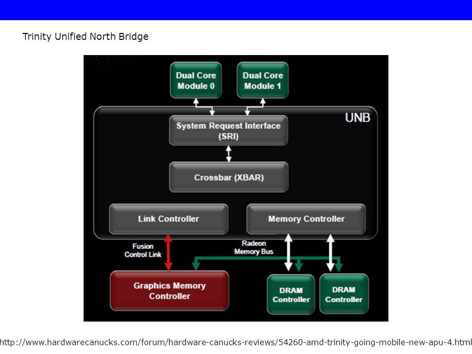
Trinity’s Unified North Bridge []

59
3.2.6 AMD’s Piledriver-based Trinity desktop APU line (7)
The Comal platform that incorporates the (Piledriver-based) Trinity APU and the A70M PCH [26]
 Trinity APU and the. A70M PCH [26]")
60
3.2.7 Okostelefonok

61
3.2.7 Okostelefonok (1) 3.2.7 Smart phone platforms
Example: Texas OMAP 5 (OMAP 5430) [27]
 [27]")
62
3.2.7 Okostelefonok (2) Main features of the OMAP 5430 [27]
![3.2.7 Okostelefonok (2) Main features of the OMAP 5430 [27]](http://slideplayer.hu/slide/2131952/8/images/62/3.2.7+Okostelefonok+%282%29+Main+features+of+the+OMAP+5430+%5B27%5D.jpg "3.2.7 Okostelefonok (2) Main features of the OMAP 5430 [27]")
63
3.2.7 Okostelefonok (3) Megjegyzés
2012 novemberében Texas Instruments (TI) bejelentette, hogy kivonul a mobil eszközök (okostelefonok, táblagépek) fejlesztéséből és az OMAP családját a jövőben a beágyazott rendszerek területén (autóelektronika, robotika) fogja alkalmazni. Egyúttal AMD 1700 munkahelyet szüntetett meg [28].
 bejelentette, hogy kivonul a mobil eszközök. (okostelefonok, táblagépek) fejlesztéséből és az OMAP családját a jövőben a beágyazott. rendszerek területén (autóelektronika, robotika) fogja alkalmazni. Egyúttal AMD 1700 munkahelyet szüntetett meg [28].")
64
4. Kitekintés

65
Heterogenous multicores
4. Kitekintés (1) Kitekintés Heterogenous multicores Master/slave architectures Add-on architectures Több CPU Több gyorsító 4.1 ábra: Hetererogén többmagos processzorok várható fejlődése
 Kitekintés. Heterogenous multicores. Master/slave. architectures. Add-on. architectures. Több CPU. Több gyorsító. 4.1 ábra: Hetererogén többmagos processzorok várható fejlődése.")
66
Referenciák

67
References (1) [1]: Wright C., Henning P., Bergen B., Roadrunner Tutorial, An Introduction to Roadrunner, and the Cell Processor, Febr , [2]: Blachford N., Cell Architecture Explained, v.02, 2005, [3]: Ricker T., World's fastest: IBM's Roadrunner supercomputer breaks petaflop barrier using Cell and Opteron processors, Engadget, June , 06/09/worlds-fastest-ibms-roadrunner-supercomputer-breaks-petaflop/ [4]: NVIDIA CUDA Compute Unified Device Architecture, Programming Guide, Version 1.1, Nov , Programming_Guide_1.1.pdf [5]: RS – Intel 2009 Desktop Platform Overview, Sept. 2007, [6]: Smith S.L., Intel Roadmap Overview, IDF 2009, Sept , [7]: Smith S.L., 32nm Westmere Family of Processors, 2009, [8]: Kahn O., Piazza T., Valentine B.: Technology Insight: Intel Next Generation Microarchitecture Codename Sandy Bridge, IDF 2010, extreme.pcgameshardware.de/.../281270d bonusmaterial-pc- games-hardware sf10_spcs001_100.pdf
![References (1) [1]: Wright C., Henning P., Bergen B., Roadrunner Tutorial, An Introduction to Roadrunner,](http://slideplayer.hu/slide/2131952/8/images/67/References+%281%29+%5B1%5D%3A+Wright+C.%2C+Henning+P.%2C+Bergen+B.%2C+Roadrunner+Tutorial%2C+An+Introduction+to+Roadrunner%2C.jpg "and the Cell Processor, Febr , [2]: Blachford N., Cell Architecture Explained, v.02, 2005, [3]: Ricker T., World s fastest: IBM s Roadrunner supercomputer breaks petaflop barrier using. Cell and Opteron processors, Engadget, June , 06/09/worlds-fastest-ibms-roadrunner-supercomputer-breaks-petaflop/ [4]: NVIDIA CUDA Compute Unified Device Architecture, Programming Guide, Version 1.1, Nov , Programming_Guide_1.1.pdf. [5]: RS – Intel 2009 Desktop Platform Overview, Sept. 2007, [6]: Smith S.L., Intel Roadmap Overview, IDF 2009, Sept , [7]: Smith S.L., 32nm Westmere Family of Processors, 2009, [8]: Kahn O., Piazza T., Valentine B.: Technology Insight: Intel Next Generation Microarchitecture. Codename Sandy Bridge, IDF 2010, extreme.pcgameshardware.de/.../281270d bonusmaterial-pc- games-hardware sf10_spcs001_100.pdf.")
68
References (2) [9]: Intel Sandy Bridge Review, Bit-tech, Jan. 3 2011,
[10]: 2nd Generation Intel Core Processor Family Desktop, Datasheet, Vol.1, Jan. 2011, [11]: George V., Piazza T., Jiang H., Technology Insight: Intel Next Generation Microarchitecture, Codename Ivy Bridge, IDF 2011, SPCS005 [12]: Athow D., Picture : Ivy Bridge vs Sandy Bridge GPU Die Sizes Compare, ITProPortal, April , bridge-gpu-die-sizes-compared/ [13]: AMD Completes ATI Acquisition and Creates Processing Powerhouse, Oct , [14]: AMD Torrenza and Fusion together, Metal Ghost, March , torrenza-and-fusion-together [15]: Rivas M., AMD 2007 Financial Analyst Day Presentation, Dec [16]: AMD Financial Analyst Day 2008, Nov , [17]: Hruska J., AMD Fusion now pushed back to 2011, Ars Technica, Nov ,
![References (2) [9]: Intel Sandy Bridge Review, Bit-tech, Jan ,](http://slideplayer.hu/slide/2131952/8/images/68/References+%282%29+%5B9%5D%3A+Intel+Sandy+Bridge+Review%2C+Bit-tech%2C+Jan+%2C.jpg "[10]: 2nd Generation Intel Core Processor Family Desktop, Datasheet, Vol.1, Jan. 2011, [11]: George V., Piazza T., Jiang H., Technology Insight: Intel Next Generation Microarchitecture, Codename Ivy Bridge, IDF 2011, SPCS005. [12]: Athow D., Picture : Ivy Bridge vs Sandy Bridge GPU Die Sizes Compare, ITProPortal, April , bridge-gpu-die-sizes-compared/ [13]: AMD Completes ATI Acquisition and Creates Processing Powerhouse, Oct , [14]: AMD Torrenza and Fusion together, Metal Ghost, March , option=com_content&view=article&id=233:amd- torrenza-and-fusion-together. [15]: Rivas M., AMD 2007 Financial Analyst Day Presentation, Dec [16]: AMD Financial Analyst Day 2008, Nov , [17]: Hruska J., AMD Fusion now pushed back to 2011, Ars Technica, Nov ,")
69
References (3) [18]: Intel cans 45nm “Auburndale” and “Havendale” Fusion CPUs!, Jan , and-havendale-fusion-cpus/ [19]: Wikipedia, Turion, [20]: Foley D., AMD’s „LLANO” Fusion APU, Hot Chips 23, Aug , HC Llano-Fusion-Foley-AMD.pdf [21]: AMD A-Series APU, EMEA Press Call, June , [22]: Kirsch N., AMD Llano A-Series APU Sabine Notebook Platform Review, Legit Reviews, June , [23]: Chiappetta M., AMD A Llano APU and Lynx Platform Preview, Hot Hardware, June , Platform-Preview/?page=2 [24]: Walrath J., AMD, Vishera, and Beyond: New Design Philosophy Dictates a Faster Pace, PC Perspective, July , Beyond-New-Design-Philosophy-Dictates-Faster-Pace/How-Does-Vishera [25]: Wasson S., AMD's A M 'Trinity' APU reviewed, Tech Report, May ,
![References (3) [18]: Intel cans 45nm Auburndale and Havendale Fusion CPUs!, Jan ,](http://slideplayer.hu/slide/2131952/8/images/69/References+%283%29+%5B18%5D%3A+Intel+cans+45nm+Auburndale+and+Havendale+Fusion+CPUs%21%2C+Jan+%2C.jpg "and-havendale-fusion-cpus/ [19]: Wikipedia, Turion, [20]: Foley D., AMD’s „LLANO Fusion APU, Hot Chips 23, Aug , HC Llano-Fusion-Foley-AMD.pdf. [21]: AMD A-Series APU, EMEA Press Call, June , [22]: Kirsch N., AMD Llano A-Series APU Sabine Notebook Platform Review, Legit Reviews, June , [23]: Chiappetta M., AMD A Llano APU and Lynx Platform Preview, Hot Hardware, June , Platform-Preview/ page=2. [24]: Walrath J., AMD, Vishera, and Beyond: New Design Philosophy Dictates a Faster Pace, PC Perspective, July , Beyond-New-Design-Philosophy-Dictates-Faster-Pace/How-Does-Vishera. [25]: Wasson S., AMD s A M Trinity APU reviewed, Tech Report, May ,")
70
References (4) [26]: Paul D., Meet the new AMD APUs Series A-2nd generation “Trinity”, TechNews, May , [27]: OMAP 5 Mobile Applications Platform, Product Bulletin, Texas Instruments, 2011, [28]: Hibben M., Texas Instruments and the Big Chip Maker Anachronism, Nov , anachronism/16680/
![References (4) [26]: Paul D., Meet the new AMD APUs Series A-2nd generation Trinity , TechNews, May ,](http://slideplayer.hu/slide/2131952/8/images/70/References+%284%29+%5B26%5D%3A+Paul+D.%2C+Meet+the+new+AMD+APUs+Series+A-2nd+generation+Trinity+%2C+TechNews%2C+May+%2C.jpg "[27]: OMAP 5 Mobile Applications Platform, Product Bulletin, Texas Instruments, 2011, [28]: Hibben M., Texas Instruments and the Big Chip Maker Anachronism, Nov , anachronism/16680/")
71
Köszönöm a figyelmet!

72
GNB: Graphics North Bridge
RMB: Radeon Memory Bus

73
Trinity Unified North Bridge
74
http://www. hardwarecanucks
75
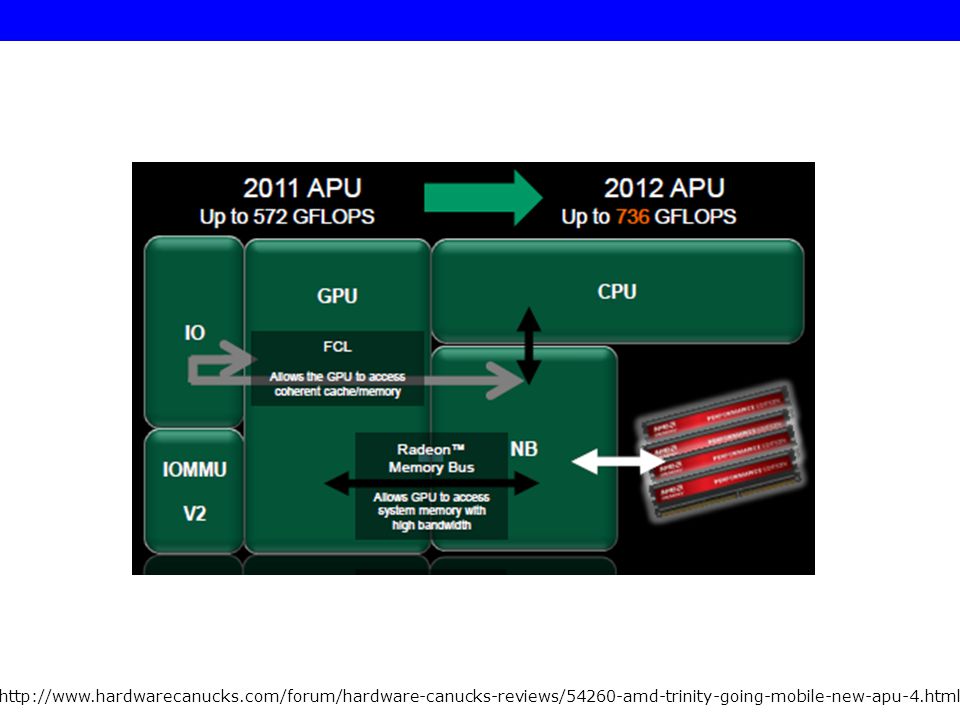
The links between each section of the APU follow in the same footsteps as the previous generation but AMD has refined certain interconnects with the goal of speeding up information transfers. The AMD Fusion Compute Link is still considered to be a medium bandwidth connection which manages the complex interaction between the onboard GPU, the CPU’s cache and the system memory. Unlike in the past, AMD has finally refined this interconnect, giving the GPU direct access to a coherent memory space while the CPU can now directly access the GPU’s dedicated framebuffer if needed. This is one of the primary reasons why Trinity’s theoretical data throughput has jumped from 572 GFLOPS to 736 GFLOPS. The Radeon Memory Bus on the other hand is the all-important link between the onboard graphics coprocessor and the primary on-chip memory controller. Rather than acting like a traffic cop (a la Fusion Compute Link) which tries to direct the flow of information, this memory bus is all about the GPU having unhindered high bandwidth access to the system’s memory controllers. In the previous generations of AMD IGPs, before Llano came around, the Northbridge’s graphics processor had to jump through a series of hoops before gaining access to onboard memory which is partially why 128MB of “SidePort” memory was sometimes added. However, the APU’s single chip, all in one solution allows for the elimination of many potential bottlenecks.
76
Trinity This unit adds virtual address access discrete graphics, allowing an external GPU to directly access the same virtual address space as the CPU through page tables. As you can imagine, this is a key part of the programming model for AMD’s Heterogeneous Systems Architecture (HSA).
.")
Hasonló előadás


 technológia lehetőségei a pénzügyi szektorban.>")


Auto-indexing enabled b)Auto-indexing disabled c)Nem eldönthető 1.>")


>")

